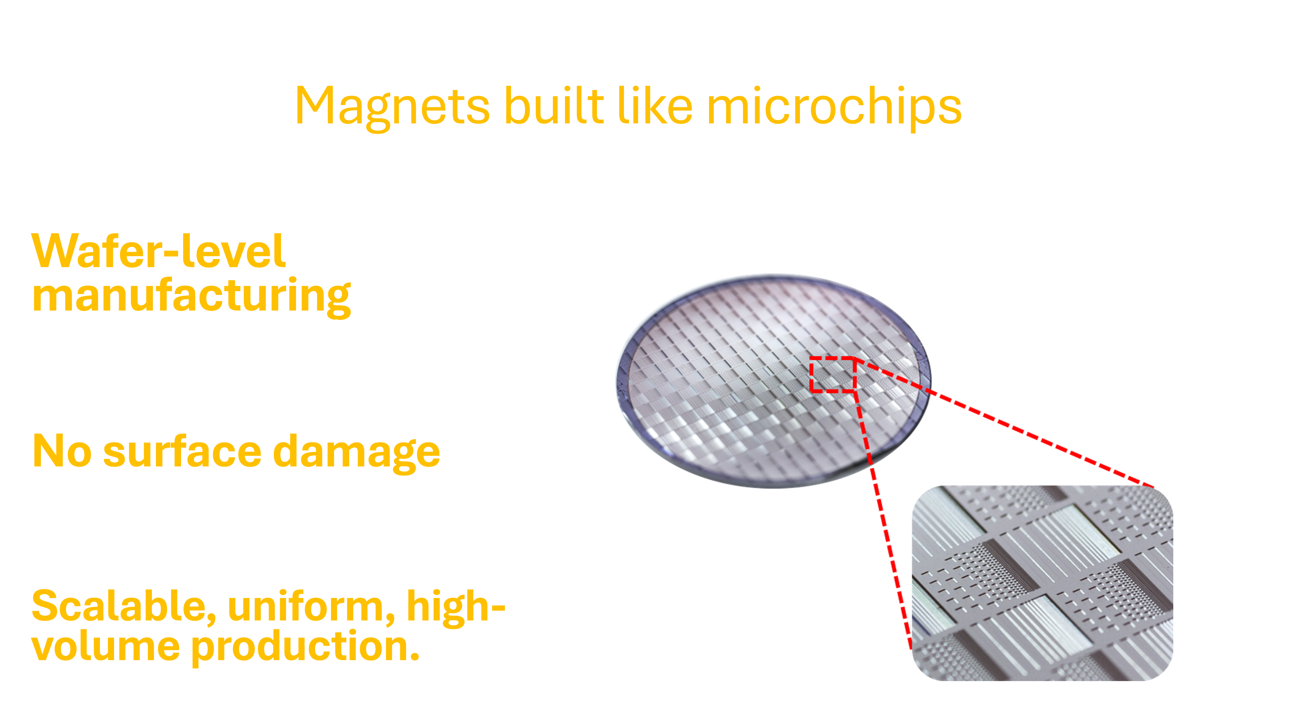
MicromagnetS
for high-performance
miniaturized devices.

About us

Magnetfab is a supplier of high-performance micromagnets for the semiconductor and microelectronics industries. We offer magnets as small as a grain of sand, which corresponds to a size reduction of more than 10x compared to what is currently available on the market.

At the same time, our micromagnets are as strong as the big magnets used in Tesla's model 3 engine or in CERN's particle accelerators. In addition to addressing our customers' need for miniaturization, we offer a wafer-level solution that allows for automated manufacturing processes.

Technology

Magnetfab’s patented technology is based on more than a decade of research conducted at Institut Néel - CNRS Grenoble, which is one of the world’s top research institutions in the field of magnetism.

Unlike the traditional fabrication approach for magnets that relies on powder metallurgy, we produce micromagnets by means of sputtering, a technique which consists in depositing thin film layers that is widely used for manufacturing optical coatings and semiconductor devices.

Utilizing state-of-the-art microfabrication equipment within a controlled clean-room environment, we can achieve microscale precision in patterning our sputtered magnetic films. This capability enables us to produce thousands of micromagnets with unrivaled uniformity and submicron-level shape control, all seamlessly integrated onto a single wafer.

What sets our magnetic films apart is that they consist of Neodymium Iron Boron (NdFeB), an alloy based on rare-earth elements known for possessing the highest energy density among all known magnetic materials. Notably, NdFeB is the very same permanent magnet material employed in over 90% of contemporary electric vehicle traction motors. The robust and strong static magnetic field of NdFeB magnets even finds application in guiding and shaping beams of particles moving at nearly the speed of light within particle accelerators.

Wafer-level micromagnets.
a) Example of a 100 mm Si wafer containing rectangular-shaped micromagnets with a thickness of 50 µm. The smallest magnets have lateral dimensions as small as 20 µm.
b) Magnified picture from the wafer.
c) Cross-section.
d) Magnetic field measured near the surface of a sample.

The table below summarizes the main specifications of our micromagnets:

Precision for shape Control ≈ 1 μm in lateral dimensions.
≈ 0.1 μm in thickness.
Remanence Br Up to 1.3 T for out-of-plane operation.
0.6 T for in-plane operation.
Coercivity Hci 1600 kA/m (2 T). Can be increased to 3T by composition tuning.
Variations in Br et Hci ≈ 1% on a single wafer
Maximum magnet thickness tmax (on Si) tmax ≈ 50 μm
Minimum lateral dimensions ≈ 50 μm for tmax. If a magnet thickness of 10 μm is sufficient, then the lateral size can be reduced to 10 μm.
Maximum lateral dimensions ≈ 300μm for tmax. If a magnet thickness of 10-20 μm is sufficient, then one can implement lateral dimensions of several millimeters and beyond.
Substrate material Typically Si. Other materials also possible, such as metals (e.g. Ti), glass, sapphire.
Substrate size Currently we work with 100 mm Si wafers for prototype fabrication. Scaling up to 200 mm sized wafers planned for 2025 onwards.
Maximum operating temperature for the magnets (i.e. temperature up to which magnetic properties are reversible) ≈ 80 °C. Can be increased by composition tuning.

Applications

Just as LEDs have revolutionized lighting and transistors have empowered computing, micromagnets hold the promise of disrupting microsystems, most prominently represented by microelectromechanical systems (MEMS). The importance of using permanent magnets in microsystems lies in their ability to enable miniaturization, energy efficiency, and precise control of magnetic fields at the microscale. This opens up a wide range of applications in fields like in medtech, portable consumer devices, microfluidics, robotics, sensing, and in quantum technology, where the integration of magnetic functionality is essential for achieving desired performance and functionality in micro-sized devices.

Microspeakers
Miniaturized loudspeakers for hearing aids and true wireless stereo (TWS) earbuds.
Cell phone camera
Actuators for autofocus and optical image stabilization.
Tactile sensors
Giving the sense of touch tofor prosthetics and to robotic systems.
Augmented reality
Scanning MEMS micromirrors for making ultra-compact projection displays.
Automotive position sensors
Contactless and robust position sensing of moving parts such as valves and the motor.
Haptic feedback
Providing high-resolution tactile feedback, e.g. when touching a smartwatch.
Magnetic field sensors
For measuring extremely weak biomedical signals, e.g. from the heart and the brain.
Microfluidics
Micropumps, magnetic cell separation and droplet manipulation.

Prototypes

Samples of micromagnets with generic shapes (square/rectangular/circular) can already be purchased for testing purposes. Customized shapes are also possible, provided that they are compatible with our design rules. Our wafer-level microfabrication approach facilitates a high design freedom, allowing the realization of the simplest shapes as well as complex patterns, as shown in the examples here below.

In case of interest, please send us an email with your request.
Examples of micromagnet structures that can be realized with Magnetfab’s manufacturing process.

Missions

Magnetfab operates as a micromagnet foundry and supplier. Our mission is to assist our customers in the creation of more compact, energy-efficient, and dependable devices by means of micromagnet-based technology. Through our microtechnology-driven approach to high-volume manufacturing, we minimize the usage of rare-earth materials in electronic devices and lessen the environmental impact of magnet production compared to traditional approaches. We are convinced that micromagnets will be at the heart of a plethora of future microdevices that will improve many people’s lives through a broad range of application areas, and our ambition is to trigger this magnetic revolution.

Contact

Company address coming soon.

For any types of requests or questions, please send us an email.
Send email

Partners & Supporters

LEGAL NOTICE
www.magnetfab.com is a publication of Magnetfab, France.
Publication director : Milan CALIC

The links present on ths site can direct the visitor to the sites which are commercial or institutional site whose content engages the responsability of the person in charge of the publication of each site.

INTELLECTUAL PROPERTY
The site is protected by intellectual property rights and in particular copyright. The use of all or part of the site, in particular by downloading, reproduction, transmission or representation on any medium and by any process, for purposes other than for personal and private use for a non-commercial purpose is strictly prohibited. All corporate names, brands and distinctive signs reproduced on the site are also protected under trademark law. The reproduction or representation of all or part of one of the aforementioned signs must be subject to the prior written authorization of the holder of the marks and signs. In general, any unauthorized reproduction or representation of brands, logos, drawings, models, literary, musical, audiovisual, photographic works and more generally of any element likely to be protected by an intellectual property right accessible on the site is prohibited and would constitute an infringement within the meaning of articles L335-2 and following of the Intellectual Property Code, unless this reproduction or representation is exclusively reserved for strictly personal and private use.
WebDesign: www.elodieguivarch.com
Development: MVP
Cookies
There are no cookies in this website, except PHP session cookie.
No personal data is recorded, nor transmitted to any third party.